TEL:+86 132 6656 7067


Artificial intelligence infrastructure depends on moving enormous volumes of data between processors, memory, accelerators, and network systems. As AI models grow and computing architectures become more distributed, the performance of data connections is becoming just as important as the processing capability of individual chips.
Traditional electrical interconnects remain essential for communication over short distances, but their power consumption, signal integrity, and reach become increasingly challenging as bandwidth requirements rise. Optical Input/Output (Optical I/O) technology addresses these limitations by bringing optical communication closer to computing chips. Instead of relying entirely on electrical signals to travel across longer connections, Optical I/O converts data into optical signals near the processing device and transmits it through fiber.
This approach creates new opportunities for chip-to-chip communication, accelerator scaling, memory expansion, and high-performance AI data center architecture.
1. What Is Optical I/O Technology?
Optical I/O refers to technologies that use optical signals to transmit data between chips, chiplets, processors, memory resources, or other computing components. Electrical signals are converted into optical signals near the source, transmitted through optical waveguides or fiber, and converted back into electrical signals at the receiving end.
Unlike conventional pluggable optical transceivers, which typically connect through external switch or server ports, Optical I/O aims to place optical interfaces much closer to the computing silicon. This reduces the distance that high-speed electrical signals must travel before entering the optical transmission path.
1.1 The Basic Optical I/O Signal Path
An Optical I/O system generally contains several functional elements:
Electrical interface: Receives data from the processor, switch ASIC, or chiplet.
Electronic interface circuitry: Prepares electrical signals for electro-optical conversion.
Photonic integrated circuit (PIC): Uses optical components such as modulators, waveguides, and photodetectors to transmit or receive optical signals.
Optical transmission path: Carries data through optical waveguides or fiber.
Optical receiver: Converts incoming optical signals back into electrical signals for the destination device.
The exact architecture varies by implementation. Some systems use separate optical I/O chiplets, while others integrate photonic components with electronic dies through advanced packaging.
1.2 Optical I/O Is Not the Same as a Pluggable Transceiver
Both technologies perform electrical-to-optical and optical-to-electrical conversion, but their integration points and intended applications are different.
| Technology | Integration Location | Primary Function |
|---|---|---|
| Pluggable optical transceiver | Switch or server front panel | Connects equipment through external optical links |
| On-board optics (OBO) | On the system circuit board | Moves optical conversion closer to the host ASIC |
| Near-packaged optics (NPO) | Close to the electronic package | Shortens high-speed electrical connections to optical interfaces |
| Co-packaged optics (CPO) | Integrated within or closely associated with the ASIC package | Combines switching or computing silicon with nearby optical engines |
| Optical I/O chiplet | Near or within a multi-chip package | Provides optical input/output for chip-to-chip or system-level communication |
These categories can overlap. Optical I/O describes a function and interface approach, while CPO and NPO describe ways of integrating optical components into a system. An Optical I/O chiplet may be used in a co-packaged architecture, but the terms are not interchangeable.
2. Why AI Infrastructure Needs Optical I/O
AI workloads create intensive communication between GPUs, CPUs, memory systems, and network devices. During distributed model training, accelerators exchange parameters, gradients, and intermediate results. During inference, processors may need to access large model weights and distributed memory resources with predictable latency.
As the number of accelerators increases, the communication infrastructure must scale alongside computing capacity. Adding more processing units without improving their interconnects can create bottlenecks that limit overall system performance.
2.1 Electrical Interconnects Face Increasing Bandwidth Pressure
Electrical connections are highly effective for short-distance communication, particularly within a processor package or between nearby components. However, as data rates increase, electrical channels become more sensitive to insertion loss, crosstalk, reflections, and frequency-dependent signal distortion.
Longer electrical paths may require additional signal-conditioning circuitry, increasing system complexity and power consumption. These limitations become more significant when multiple high-speed connections must operate simultaneously in a densely integrated AI system.
2.2 Data Movement Is Becoming a System-Level Bottleneck
Modern AI infrastructure is not limited by compute performance alone. Data must continuously move between processing units and memory resources. If communication bandwidth is insufficient, accelerators may spend more time waiting for data instead of executing calculations.
Optical I/O provides a potential way to increase communication bandwidth and extend connection reach without requiring every high-speed data path to remain electrical.
3. How Optical I/O Improves AI Chip Connectivity
Optical I/O changes the physical location of signal conversion. By placing optical interfaces closer to the source of data, system designers can reduce the length and complexity of high-speed electrical connections.
3.1 Shorter Electrical Paths
In conventional architectures, high-speed electrical signals travel from a processor or switch ASIC through package traces, PCB routing, connectors, and eventually to an optical module. Each section of the electrical channel introduces losses and signal-integrity constraints.
Optical I/O moves the electrical-to-optical conversion point closer to the computing silicon. Once the data has been converted into optical form, it can travel through fiber or optical waveguides with lower propagation loss over suitable distances.
3.2 Higher Bandwidth Density
Optical communication can support multiple high-speed channels within a compact fiber or waveguide arrangement. Wavelength-division multiplexing (WDM) can further increase aggregate capacity by carrying multiple optical wavelengths through the same transmission medium.
This capability is valuable for AI systems that need to connect many processing components without allowing electrical connector density and PCB routing to become major physical constraints.
3.3 Potential Improvements in Energy Efficiency
High-speed electrical signaling over longer channels may require substantial power for drivers, equalization, and retiming. Optical I/O can reduce some of these electrical transmission requirements by converting signals closer to the source.
However, optical communication is not automatically lower power in every implementation. Lasers, modulators, drivers, receivers, control circuits, and thermal management all contribute to total energy consumption. System-level measurements are necessary to determine the actual energy efficiency.
4. Optical I/O Applications Across AI Infrastructure
Optical I/O can support multiple communication layers in an AI data center. Its role extends beyond conventional switch-to-switch optical networking and may eventually reach the connections between processors and memory systems.
4.1 GPU-to-GPU Connectivity
Large AI systems use multiple GPUs or other accelerators to distribute computing workloads. These devices exchange data during training and inference, making high-bandwidth communication essential.
Optical I/O could help extend high-bandwidth connections between accelerator components when conventional electrical links become difficult to scale. Depending on the architecture, optical links may connect chiplets within a package, processors across a board, or computing resources across larger physical distances.
Optical I/O does not replace every existing GPU interconnect. Short-reach electrical technologies such as high-speed die-to-die links remain attractive within tightly integrated packages. Optical links become more relevant as communication distance and aggregate bandwidth requirements increase.
4.2 CPU-to-GPU Communication
AI servers commonly combine CPUs, GPUs, memory, storage, and network interfaces. These components exchange data through a combination of internal buses, PCIe connections, high-speed electrical interfaces, and external network links.
As accelerator platforms become more complex, optical I/O may provide additional connectivity options between processing components or chiplet-based subsystems. This could help system designers build larger and more flexible computing architectures.
4.3 Processor-to-Memory Connectivity
Memory bandwidth and capacity are critical to AI performance. High-bandwidth memory (HBM) provides extremely high data rates over short physical connections within advanced packages. However, scaling memory capacity and connecting distributed memory resources introduce additional architectural challenges.
Optical I/O could support future memory expansion and memory disaggregation by connecting processors to memory resources beyond the immediate package. Optical links may provide longer reach and higher aggregate bandwidth for these connections.
This does not mean optical I/O will directly replace the short-reach electrical interfaces used by HBM. Instead, it may complement existing memory technologies by supporting communication between larger groups of processors and memory resources.
4.4 Switch-to-Processor Connectivity
AI infrastructure also depends on high-speed communication between compute nodes and network switches. Optical I/O can help bring optical connectivity closer to switching or processing silicon, potentially reducing the electrical distance between the ASIC and optical transmission interface.
This is closely related to the development of CPO and other advanced optical integration approaches. For external network connections, pluggable 800G and 1.6T optical transceivers will continue to serve important applications as supported by the host platform.
5. Optical I/O, Silicon Photonics, and CPO
Optical I/O depends on advances in photonic integration and packaging technologies. Silicon photonics, photonic integrated circuits, and co-packaged architectures are important parts of this development.
5.1 Silicon Photonics
Silicon photonics uses semiconductor manufacturing processes to integrate optical functions onto photonic chips. These chips can contain waveguides, modulators, optical couplers, and photodetectors, depending on the design.
Silicon photonics can help reduce the size of optical components and support higher levels of integration. It also provides a pathway for combining photonic devices with electronic integrated circuits through advanced packaging.
5.2 Optical I/O Chiplets
An Optical I/O chiplet is a dedicated optical interface component designed to work alongside a host processor, accelerator, or other electronic chip. Rather than placing all optical functions inside the main computing die, designers can use a separate photonic component connected through a suitable package interface.
This chiplet approach offers flexibility in system design. Compute, memory, electronic interface, and photonic functions can be developed as separate components and combined through advanced packaging.
Potential advantages include:
More flexible integration of photonic and electronic components.
Higher aggregate bandwidth between computing resources.
Reduced dependence on long high-speed electrical traces.
Support for modular chiplet-based computing architectures.
New opportunities for connecting distributed processors and memory.
5.3 Co-Packaged Optics
Co-Packaged Optics integrates optical engines close to or within the same package as a high-performance electronic chip, such as a switch ASIC. The goal is to reduce the distance that high-speed electrical signals travel before optical conversion.
In AI infrastructure, CPO is particularly relevant to high-capacity switches and future computing platforms that require many high-speed optical connections. It can help address the power and signal-integrity challenges associated with conventional front-panel optical interfaces.
Optical I/O and CPO are related but serve different levels of description. Optical I/O identifies the optical communication interface, while CPO identifies a packaging and integration approach that can implement that interface.
5.4 The Evolution of Optical Integration
| Architecture | Optical Integration Position | Main Design Objective |
|---|---|---|
| Pluggable optics | Front-panel module | Flexible external optical connectivity |
| On-board optics | System circuit board | Shorter electrical connections to optical interfaces |
| Near-packaged optics | Near the electronic package | Reduce high-speed electrical channel length |
| Co-packaged optics | Within or adjacent to the ASIC package | Integrate optical engines with high-performance silicon |
| Chiplet-level Optical I/O | Within advanced multi-chip packages | Enable optical communication between computing components |
This progression is not a universal replacement sequence. Different architectures can coexist because they address different distances, bandwidth requirements, serviceability needs, and system costs.
6. Optical I/O and the Future of AI Network Architecture
As AI clusters expand, network architecture must support communication at several physical scales. Optical I/O may help extend optical connectivity from conventional data center links toward rack-level and chip-level communication.
6.1 Scale-Up Connectivity
Scale-Up networks connect accelerators within a tightly integrated computing system. Their purpose is to provide high-bandwidth communication between processing units that cooperate on the same workload.
Electrical interconnects remain important for short connections within packages and servers. Optical I/O could extend the scale-up architecture beyond some of these traditional electrical boundaries, allowing larger groups of computing resources to communicate through optical paths.
6.2 Scale-Out Connectivity
Scale-Out networks connect multiple servers and racks to build large AI clusters. Ethernet and InfiniBand switching systems, together with optical transceivers and fiber links, form important parts of this architecture.
Optical I/O can complement these technologies by bringing optical interfaces closer to switch or processor silicon. Meanwhile, conventional pluggable modules continue to provide modular connections between network devices.
6.3 Scale-Across Connectivity
Scale-Across architectures connect AI resources across data halls, buildings, or separate facilities. These systems require optical links with appropriate reach, capacity, latency, and reliability.
Optical I/O at the chip or package level does not replace long-distance data center interconnect technologies. Instead, it can complement external optical networking by improving communication within computing systems before traffic reaches the broader network.
7. Technical Challenges of Optical I/O Deployment
Although Optical I/O offers significant potential, commercial deployment requires solving several engineering and manufacturing challenges.
7.1 Thermal Management
AI processors and high-performance electronic components generate substantial heat. Optical devices such as lasers, modulators, and photodetectors also have temperature-dependent operating characteristics.
Integrating photonic components close to high-power processors makes thermal design particularly important. Temperature changes can affect optical performance, wavelength stability, and overall system reliability.
7.2 Optical Packaging and Alignment
Optical coupling requires precise alignment between photonic components, waveguides, and fiber connections. Manufacturing processes must maintain suitable alignment and coupling efficiency while supporting high-volume production.
Advanced packaging techniques, optical connectors, fiber attach processes, and automated testing are important for improving consistency and reducing assembly complexity.
7.3 Laser Integration and Reliability
Optical systems require suitable light sources. Depending on the architecture, lasers may be integrated with the photonic device or supplied through an external laser source.
External laser architectures can separate the light source from heat-sensitive components, but they introduce additional optical connections and system-level design considerations. Laser reliability, optical coupling, monitoring, and serviceability must all be addressed.
7.4 Manufacturing Cost and Yield
Optical I/O combines semiconductor electronics, photonic devices, packaging, and fiber assembly. Each manufacturing stage can affect final product yield and cost.
High-volume deployment requires repeatable assembly, reliable testing, standardized interfaces, and supply-chain maturity. These factors will influence how quickly Optical I/O moves from specialized systems into broader AI infrastructure.
7.5 Standardization and Interoperability
Different vendors may use different optical interfaces, electrical chiplet connections, laser arrangements, and packaging architectures. Interoperability is therefore an important consideration.
Industry standards and common interface specifications can help improve compatibility between components and reduce dependence on proprietary system designs.
8. Optical I/O Compared with Traditional Optical Connectivity
Optical I/O does not eliminate the need for conventional optical transceivers, AOC cables, or other fiber-based connectivity. These technologies serve different parts of the data center architecture.
| Connectivity Type | Typical Position | Primary Application | Key Consideration |
|---|---|---|---|
| Pluggable optical transceiver | Equipment front panel | Switch-to-switch and server-to-switch links | Modularity and optical reach |
| AOC | Between external equipment ports | Integrated short- and medium-reach optical cabling | Fixed cable assembly and supported reach |
| DAC | Between nearby equipment ports | Short-reach electrical connections | Electrical channel limits |
| AEC | Between nearby equipment ports | Active electrical connections with signal conditioning | Power and host compatibility |
| Optical I/O | Near or within computing packages | Chip-to-chip and processor-level optical communication | Integration, thermal design, and packaging |
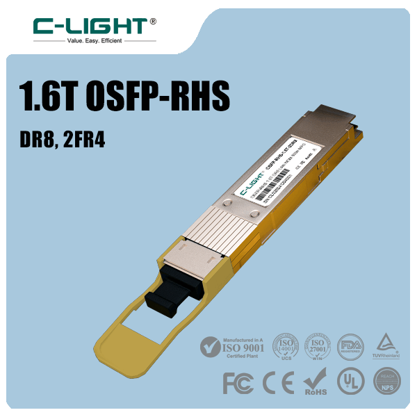
For external network connections, C-LIGHT provides optical connectivity products including 800G QSFP-DD, 800G OSFP, and 1.6T OSFP-RHS optical transceivers. These pluggable products address equipment-level optical links and should be distinguished from chip-level Optical I/O components.
9. What Optical I/O Means for Future AI Infrastructure
The long-term importance of Optical I/O is its potential to make optical communication a more integrated part of computing architecture rather than a technology used mainly at external network ports.
Several developments are likely to shape this transition:
Higher chip-to-chip bandwidth: Optical interfaces may support communication between larger groups of processors and chiplets.
More flexible computing systems: Chiplet architectures can combine compute, memory, and photonic functions in different configurations.
Expanded memory connectivity: Optical links may support future memory expansion and disaggregated memory architectures.
Lower electrical channel complexity: Moving optical conversion closer to the source can reduce the distance traveled by high-speed electrical signals.
New system-level designs: Computing, memory, networking, and photonics may be co-designed as parts of one integrated infrastructure.
These developments are still progressing through research, engineering validation, and commercial implementation. Optical I/O should therefore be viewed as an evolving technology rather than a universal replacement for current electrical and optical interconnects.
10. Conclusion
Optical I/O technology addresses one of the major challenges facing next-generation AI infrastructure: moving data efficiently between increasingly powerful computing components. By placing optical interfaces closer to processors and other electronic devices, it can help increase bandwidth density, extend communication reach, and reduce some of the limitations associated with high-speed electrical channels.
Its development is closely connected to silicon photonics, optical I/O chiplets, advanced packaging, NPO, and CPO. Together, these technologies create new possibilities for GPU connectivity, chip-to-chip communication, memory expansion, and high-performance data center networking.
Conventional pluggable optical transceivers, DAC, AEC, and AOC solutions will continue to serve important applications across external network connections. As AI systems evolve, the most effective infrastructure will combine electrical and optical technologies according to distance, bandwidth, power, and system integration requirements.
 >

 >
 >
 >
 >
 >
 >
 >