TEL:+86 132 6656 7067


1. The AI Era Is Driving a Networking Revolution
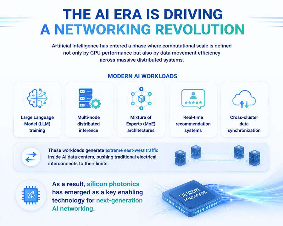
Artificial Intelligence has entered a phase where computational scale is defined not only by GPU performance but also by data movement efficiency across massive distributed systems.
Modern AI workloads include:
Large Language Model (LLM) training
Multi-node distributed inference
Mixture of Experts (MoE) architectures
Real-time recommendation systems
Cross-cluster data synchronization
These workloads generate extreme east-west traffic inside AI data centers, pushing traditional electrical interconnects to their limits.
As a result, silicon photonics has emerged as a key enabling technology for next-generation AI networking.
2. What Is Silicon Photonics?
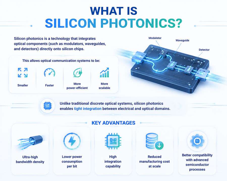
Silicon photonics is a technology that integrates optical components (such as modulators, waveguides, and detectors) directly onto silicon chips.
This allows optical communication systems to be:
Smaller
Faster
More power-efficient
More scalable
Unlike traditional discrete optical systems, silicon photonics enables tight integration between electrical and optical domains.
Key Advantages:
Lower power consumption per bit
Ultra-high bandwidth density
High integration capability
Reduced manufacturing cost at scale
Better compatibility with advanced semiconductor processes
3. Why Silicon Photonics Is Critical for AI Networking
3.1 Bandwidth Scaling Beyond 400G and 800G
AI data centers are rapidly moving from:
400G → mainstream deployment
800G → high-performance AI fabric
1.6T → next-generation architecture
Traditional optical technologies struggle to scale efficiently beyond 800G due to:
Power limitations
Signal integrity challenges
Physical packaging constraints
Silicon photonics provides a scalable path forward.
3.2 Power Efficiency in Hyperscale AI Clusters
Modern GPU clusters can reach:
40kW–100kW per rack
Networking power consumption becomes a critical bottleneck.
Silicon photonics significantly reduces:
Electrical-to-optical conversion loss
DSP overhead in high-speed transceivers
Total energy per transmitted bit
This is essential for sustainable AI infrastructure.
3.3 Enabling Dense AI Fabric Architectures
AI training requires:
Massive parallel GPU communication
Ultra-low latency synchronization
High bisection bandwidth
Silicon photonics enables:
Higher port density per switch
Reduced front-panel congestion
More compact AI switching systems
4. Silicon Photonics and Optical Interconnect Evolution
Silicon photonics is not replacing existing optical technologies overnight—it is accelerating their evolution.
Current AI Networking Stack:
DAC for short-reach in-rack connections
AOC for cross-rack flexibility
Traditional optical transceivers for leaf-spine and DCI
Silicon photonics for next-generation integration
C-LIGHT supports this full stack with:
400G QSFP-DD DR4 / FR4 optical modules
400G QSFP-DD AOC and DAC solutions
800G OSFP and QSFP-DD800 interconnect systems
DWDM/CWDM optical transport solutions
5. Silicon Photonics in AI Data Center Architecture
5.1 GPU Cluster Interconnect Layer
In AI training clusters, GPU-to-GPU communication is the most bandwidth-intensive workload.
Silicon photonics enables:
Faster optical modulation
Higher lane density (112G/224G evolution)
Reduced latency across fabric layers
C-LIGHT provides supporting infrastructure:
400G/800G optical modules optimized for AI fabrics
High-performance DAC/AOC interconnects for short reach
Compatibility testing for NVIDIA / Broadcom / Intel ecosystems
5.2 Leaf-Spine Network Scaling
Silicon photonics improves scalability in leaf-spine architectures by:
Increasing per-port bandwidth
Reducing switch power consumption
Enabling more compact switch designs
C-LIGHT solutions include:
400G QSFP-DD DR4 / FR4 / LR4
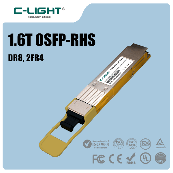
800G DR8 / 2×FR4 optical modules
High-density AI networking interconnect portfolio
5.3 Data Center Interconnect (DCI)
For multi-site AI clusters:
Silicon photonics enables efficient long-haul optical integration
Supports DWDM-based high-capacity transmission
Reduces cost per transmitted bit
C-LIGHT provides:
100G–400G DWDM optical modules
MUX/DEMUX systems
Scalable optical transport solutions for AI campuses
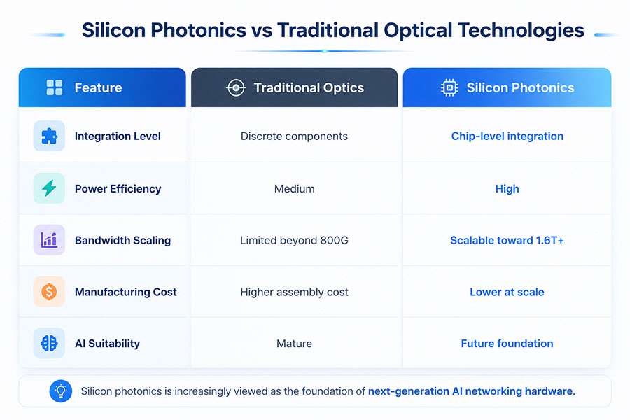
6. Silicon Photonics vs Traditional Optical Technologies
7. The Road to 1.6T and Beyond
Silicon photonics is a key enabler for the transition to:
1.6T optical interconnects
Multi-terabit AI switching systems
Ultra-dense GPU fabric architectures
Future AI systems will require:
Higher optical lane speeds
More integrated photonic-electronic co-design
Reduced power per transmitted bit
C-LIGHT is actively evolving its portfolio toward:
OSFP-XD and next-gen form factors
800G and 1.6T-ready interconnect architectures
Silicon photonics-aligned optical solutions for AI clusters
8. Why Silicon Photonics Is a Game Changer for AI
Silicon photonics is revolutionizing AI networking because it directly solves the three core challenges of modern AI infrastructure:
1. Scaling Bandwidth
Supports exponential growth from 400G → 800G → 1.6T+
2. Reducing Power Consumption
Critical for hyperscale AI data centers
3. Increasing Integration Density
Enables compact, high-performance AI fabrics
9. Conclusion
AI networking is undergoing a fundamental transformation, and silicon photonics sits at the center of this revolution.
It is not just an incremental improvement—it is a foundational technology that enables:
Ultra-high bandwidth AI clusters
Energy-efficient data center design
Scalable 1.6T+ optical interconnect architectures
While DAC, AOC, and traditional optical modules remain essential today, silicon photonics defines the future direction of AI infrastructure.
C-LIGHT supports this evolution with a complete portfolio of:
400G and 800G optical interconnect solutions
DWDM optical transport infrastructure
Next-generation AI networking readiness toward silicon photonics era
As AI continues to scale, silicon photonics will become the core enabling technology behind the next generation of intelligent computing systems.
Silicon Photonics for AI Networking FAQ
Higher bandwidth capacity
Lower power consumption
Improved signal integrity
Higher integration density
Increasing power consumption
Signal loss at higher speeds
Limited bandwidth density
Thermal management pressure
Higher transmission bandwidth
Lower energy consumption per bit
Reduced signal degradation
Better scalability for large AI clusters
| Feature | Traditional Optical Transceiver | Silicon Photonics |
| Technology | Discrete optical components | Integrated photonic circuits |
| Integration Level | Lower | Higher |
| Power Efficiency | Standard | Improved |
| Bandwidth Scalability | Limited by module design | Designed for future scaling |
| Main Application | Current optical networking | Next-generation AI infrastructure |
GPU cluster networking
High-performance computing (HPC)
Data Center Interconnect (DCI)
High-speed switch connectivity
Co-packaged optics architectures
Power efficiency
Signal quality
Network scalability
Switch bandwidth density
Replacing some electrical data transmission paths with optical communication
Reducing signal processing requirements
Improving bandwidth efficiency
Supporting higher integration density
800G optical connectivity
1.6T optical interconnects
Larger GPU clusters
Advanced CPO architectures
 >
>

 >
>
 >
>
 >
>
 >
>
 >
>
 >
>
 >
>