In the optical communication industry, especially high-rate optical modules, great attention is paid to the high performance and stable quality of the device, as the core components in the field of communication and data communication, laser diodes, optical components (OSA), optical modules and other optical components in the transmission, collection, display, storage and processing of information play a crucial role. Among them, multiple optical components in the optical module, including fiber array units, coupled lenses, optical isolators, collimators, couplers and separators, and other focusing and switching optical devices must be precisely calibrated, while each component must be highly integrated and permanently bonded to each other to ensure long-term reliability, through multiple processes throughout the production process. The need to use a variety of adhesives and thermal conductivity materials, which requires very high material expertise.
1. Chip mounting
The packaging process of optical modules Can be roughly divided into three types: TO Can, Box and COB. Among them, COB (Chip on Board) package sticks the bare chip to the interconnect substrate with conductive adhesive or non-conductive adhesive, and then performs lead bonding to achieve electrical connection and drive the chip to work. This kind of package is also widely used in data center optical modules. Conductive adhesives (silver adhesives) are widely used in the optical communication industry for chip-level assembly. The compact structure design of the optical module and the iteration of high-power chips and lasers, multiple devices gather together to generate heat dissipation challenges, and the temperature rise of the device will affect the stable operation of the chip and laser, and eventually lead to the failure of the optical module. According to statistics, the higher the operating temperature of the optical module, the higher the failure rate, so the heat dissipation capacity, working temperature, bonding performance, etc. of the conductive adhesive will affect the reliability of the chip and laser.
2. Lens coupling
Optical device coupling is to divide or combine the optical power of the same wavelength. It is mainly used to transmit signals and realize photoelectric conversion of models. It can also be understood as aligning light with certain devices, such as coupling light into an optical fiber or coupling different lights. Optical coupling is a key process in the packaging process of optical devices and optical modules, which controls the loss of optical power and affects the performance of optical modules. The laser chip emits the light, turns it into focused light through the optical lens, and introduces the Z-maximum light energy into the fiber to achieve fiber transmission. However, the optical module space is small, in order to ensure the consistency of the optical module performance, the optical fiber and the optical path must complete the high-precision coupling. Since the optical coupling accuracy is often required to be within 3 microns, the curing shrinkage, moisture absorption and thermal expansion coefficient of the glue are critical.
3, optical path packaging
The optical path adhesive is used to bond and fix the splitter plate and part of the lens surface in the optical module, and it requires good optical performance. Optical modules often run uninterrupted during the working process, especially for 400G high-rate optical modules, optical path transmission requirements, low volatiles of devices and equipment and long-term, stable and efficient operation requirements are higher. Therefore, the packaging material requires excellent bond strength, low curing shrinkage, low CTE, etc., to meet the harsh environment such as high and low temperature cycle and cold and thermal shock, to prevent the expansion or contraction of chemical materials from causing stress damage to the optical module, which affects the skew of the optical module device or excessive optical path loss.
4. Pigtail assembly
Pigtails are also called bare optical fibers. One end of the pigtails has an optical fiber connector, and the other end is a broken end of the optical fiber core. The end of the optical fiber connector is used to connect the device, and the broken end of the optical fiber core is fused with the broken end of other optical fiber cores to achieve minimum insertion loss.
5. Fill the bottom
The bottom of the BGA chip on the optical module mainboard needs to be filled with glue to seal and protect the solder joints, so that the BGA package has higher mechanical reliability. The process requires that the bottom filling glue curing speed is fast, less than 10min, high solid content, low VOC volatilization, to prevent volatiles from causing optical path abnormalities.
6. Electromagnetic shielding
With the development of high-rate optical modules in the direction of miniaturization, low power consumption, high speed, long distance and intelligence, low-rate optical modules have gradually failed to meet the daily data transmission needs, and the transmission rate requirements of data centers and telecom operators are becoming higher and higher. The higher the speed of the optical module, the higher the frequency of the electromagnetic wave radiated out, the electromagnetic environment of the optical module is complex, and the need to avoid electromagnetic interference in the work can not be ignored.
7. Thermal management
As the pace of 5G gets closer and closer, the development of user needs and data centers, low speed has slowly been unable to meet the daily data transmission needs, optical modules as the core optical electronic equipment, the two most important development directions in the future, high speed and miniaturization, will face increasing heat dissipation problems. Optical fiber communication has become the main transmission way of network information because of its advantages of large transmission capacity and good confidentiality. As one of the most important devices in optical fiber communication system, optical module is widely used in wide area network (WAN), metropolitan area network (MAN), local area network (LAN) and other fields. As a core optical electronic device, optical modules are also facing increasing requirements in terms of their complexity and diversity, two of which are important aspects, namely, high speed and miniaturization. The miniaturization of optical modules will bring one of the thorniest problems, which is heat dissipation. Too many devices are accumulated together, which will inevitably bring the heat of the device is difficult to dissipate, and the heat dissipation difficulty causes the device to heat up, resulting in changes in the working state of the chip, and in serious cases, it will cause the chip to stop working.
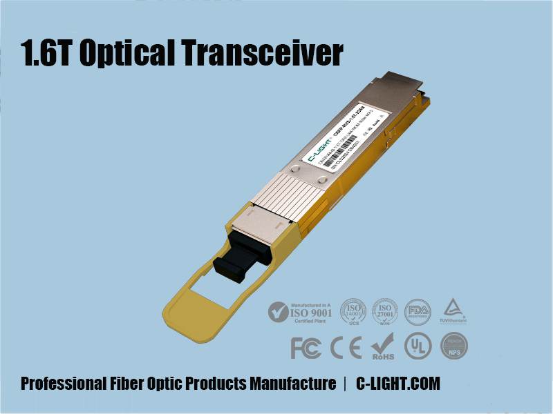
C-Light transceivers: Guaranteed Material
·All material BOMs used are subject to system control and customer supervision, eliminating arbitrary changes and replacements.
·Both core drivers and optical chip suppliers are large listed companies both domestically and internationally.
·Only authorized agents from top brands such as Murata are selected for electronic materials.
 TEL:+86 158 1857 3751




 >
>
 >
>
 >
>
 >
>
 >
>
 >
>


