PCB is an important part of optical transceiver modules. Details of design in this part are as following:
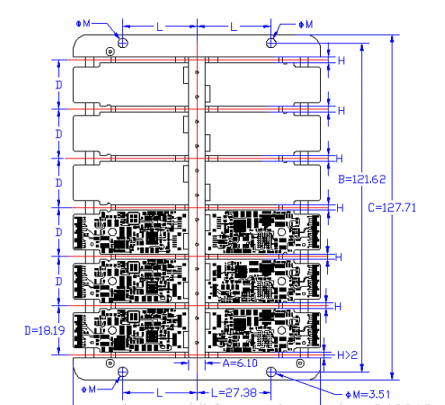
1, jigsaw mode
The miniaturized optical module PCB is recommended to be mirrored symmetrically in the center. The specific design requirements are shown in the figure below.

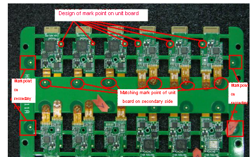
2, Mark point design
It is recommended to place two Mark points on the cell board as shown below:
Note: If there are no more than two Mark points in the cell board, but at least one Mark point is placed, and the Mark point without the copper ring can be used, and a Mark point is added on the auxiliary side to cooperate.

3, PCB connection method
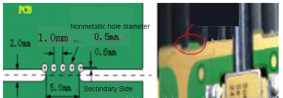
Milling groove + stamp hole design: the width of the milling groove is 2mm, the stamp hole is made of non-metallized hole, the recommended hole spacing is 1.0mm, the hole diameter is 0.5mm, as shown below:
Note: The center of the stamp hole moves toward the PCB of the optical module. It is recommended that the center of the stamp hole be ≥0.6mm from the edge of the milling slot. This can reduce the burrs on the edge of the PCB of the optical module and avoid interference with the housing, as shown in the figure below.

V-CUT connection: Refer to the general part of the PCB process design specification.
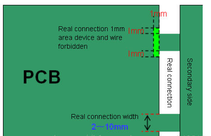
Milling groove + real connection: the width of the milling groove is 2mm, the actual connection width is 2~10mm, and the forbidden area is 1mm. The specific requirements are as follows:

The jigsaw and auxiliary block connections are preferred to use the stamp hole + milling groove method, followed by the real connection + milling slot, V-CUT connection is not recommended.
Note: V-CUT connection mode does not allow the milling cutter to split the board, but the hob splitting machine is divided into boards, the stress is large, and the layout of the optical module can not meet the requirements of the prohibition.
4, PCB process layout requirements
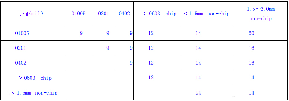
The layout distance requirements between components can be designed with reference to the following table.
In actual processing, the micro device with lower body is attached first, and then the non-chip device with higher body is attached, which can achieve good assembly;
All of the above distance values take the smallest of the pads and pads, the pads and device body, the device body and the device body.
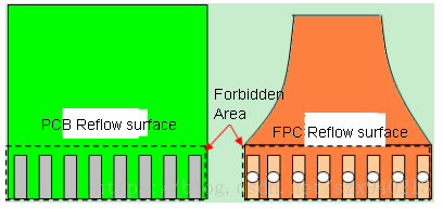
No devices are allowed in the PCB board and FPC soldering area. The specific requirements are as follows:

Hotbar process for optical device soldering: The range of the forbidden area of the hot-pressed area component is greater than 0.5mm of the press-fit operation area of the hot head, and the hot-pressed area ≥ the length of the assembly area +4mm, as shown in the following figure:

Screw-mounted optoelectronic devices: Any device and non-ground vias are prohibited within 1.5mm and at the bottom of the body, and 1.5mm non-woven devices around the fiber sheath; if it is necessary to lay out non-ground vias, it must be treated with plug holes. Increase the character oil insulation, but you must ensure that the bottom of the silk screen is not covered by the ground.
There is a gap of about 0.25 between the screw hole and the screw of the photoelectric device, plus the tolerance of the device itself is ±0.25. In addition to the tolerance of the device patch, a 1.5mm forbidden cloth is required.
1.0mm perforated vias, test pads, devices around the hand soldered optical device pads. If a hole has to be placed, the via must be fully plugged with green oil.
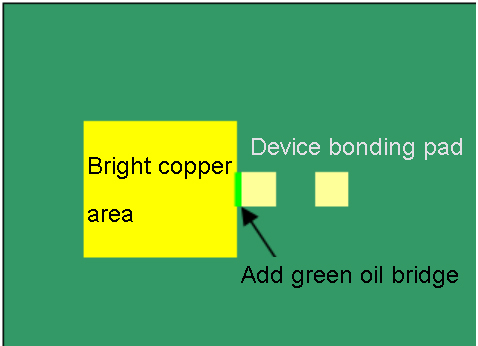
The bright copper area cannot be directly connected to the pad, and there must be solder resist isolation in the middle. The minimum width of the solder resist is 3 mil, as shown in the following figure:

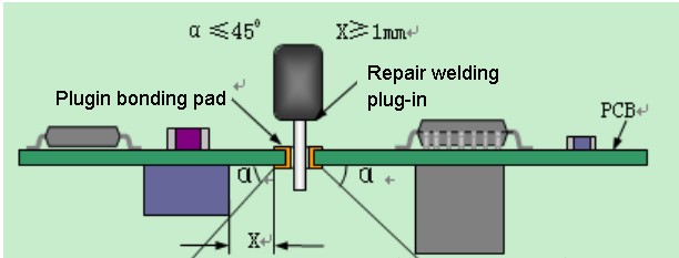
The layout distance between optical devices and between optical devices and electrical devices should meet the operating space requirements for manual soldering and maintenance, as shown in the following figure:

The optical device pins are basically hand soldered, so the layout must meet the requirements of manual soldering, otherwise it will easily hit the parts, making soldering and rework difficult.
When the optical device is deployed, the fiber-optic part cannot be inserted into the forbidden area of the fiber-optic connector, as shown in the following figure, to prevent the fiber-optic part of the optical module pigtail from being broken when the connector is plugged or unplugged.
5, PCB routing design requirements
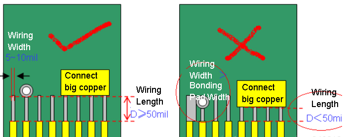
And the PCB traces Hotbar reflow disk coupled line width recommended 5 ~ 10mil; when ground requires a large area, lead length D≥50mil, as shown below:
Note: According to the test results, when the lead wire is grounded for a large area, the lead length is too small, the heat transfer is too fast during hot pressing, the process parameters are not easy to control, resulting in poor soldering, so the recommended lead length is greater than 50 mil. Thicker longer traces, connected vias, and large area copper foils dissipate quickly, resulting in uneven temperature and inconsistent soldering reliability.

6. pad design
The device is not designed to be non-thermally dissipating.
7, surface treatment
The ENIG surface treatment is preferred. For Hotbar pads, OSP surface treatment is prohibited.
8, PCB thickness design
SFP and XFP optical module PCB thickness must be 1.0mm. (SFP and XFP board thickness must be 1.0mm as specified by the MSA Agreement.)








 Your current position:

